Yocto: I/O Configuration and Device Tree Customization
Contents
Overview
Hardware devices (SoC modules, on-board peripherals etc.) and their interconnections are described in Linux O/S using data structures called Device Trees.
Compulab provides default Device Trees that match the I/O interconnections and peripheral devices implemented on the Compulab System-on-Module and on the reference carrier-board.
Customers designing a custom carrier-board will often need to make changes to the device tree in order to describe the I/O interconnections and peripheral devices specific to their design.
This article outlines the process of Device Tree customization required for making I/O configuration changes.
Board Functionality Configuration Process
Board functionality configuration will usually involve the following steps:
- Identifying configuration requirements
- Configuring required device nodes in device tree
- Configuring required pin multiplexing in device tree
Identifying Configuration Requirements
The first step in device tree customization is to identify the specific configuration or modification required in your design. This could include enabling or disabling peripherals, modifying pin assignments or configuring specific hardware-specific functionalities. To determine the customization scope, refer to the documentation of your hardware components, including the System-on-Chip (SoC), System on Module (SoM), and carrier board schematics. It is recommended to use the following Compulab resources:
- SOM technical reference manual
- Pin-mux configuration tools
- Default reference device tree
Defaut reference device tree
Compulab default reference device tree files are named according to som-name.dts template and can be found in /arch/arm64/boot/dts/compulab/ folder of BSP source. For example, default device tree file for UCM-iMX8PLUS is named ucm-imx8m-plus.dts. The default device tree file is derived from the SoC pin-multiplexing header file which is part of the SoC BSP. Pin multiplexing configuration is controlled by SoC registers. These registers are documented in detail in the SoC technical reference manual.
Configuring Device Tree Nodes
Device tree nodes are segments of the device tree that contain information about a specific hardware device. The contents of each node are dictated by the driver that is responsible for handling the hardware component.
Device tree nodes need to be modified or added when new hardware devices are added or functionality is changed.
The following documents contain detailed information about the Linux device tree and its structure:
Configuring Pin Multiplexing
Pin Selection and Allocation
The majority of ARM-based SoC pins are multi-functional and multiplexed allowing to use a single physical pin for one of several functions.
Certain functions may be available on more than one pin. Using a specific pin for a certain function will preclude using it for another peripheral module.
Carrier-board designers must select and allocate interface pins per the requirements of their design taking into account pin availability and multiplexing constraints.
Pin availability and multiplexing of Compulab System-on-Modules are described in detail in the "Signal Multiplexing Characteristics" reference manual chapter of each SOM. In addition, pin multiplexing tools can be used to simplify pin allocation process.
Modifying the device tree
The device tree segment that controls pin multiplexing will typically look as shown below:
&iomuxc {
	pinctrl-names = "default";
	pinctrl-0 = <&pinctrl_hog>;

	pinctrl_hog: hoggrp {
		fsl,pins = <
			MX8MP_IOMUXC_HDMI_DDC_SCL__HDMIMIX_HDMI_SCL	0x400001c3
			MX8MP_IOMUXC_HDMI_DDC_SDA__HDMIMIX_HDMI_SDA	0x400001c3
			MX8MP_IOMUXC_HDMI_HPD__HDMIMIX_HDMI_HPD		0x40000019
			MX8MP_IOMUXC_HDMI_CEC__HDMIMIX_HDMI_CEC		0x40000019
		>;
	};
...
};
Each pin has up to 8 multiplexed functions. To simplify selecting the pin function, NXP provides macros for each SOC with the following naming convention: <SOC>_<PIN NAME>_<PIN FUNCTION>.
For example: MX8MP_IOMUXC_NAND_READY_B__GPIO3_IO16 in which SOC = MX8MP, PIN NAME = IOMUXC_NAND_READY_B_, PIN FUNCTION = GPIO3_IO16.
Pin multiplexing registers and settings are documented in detail in each SoC reference manual that can be downloaded from the NXP website.
Each i.MX SoC has a pin config file with pin function macro definitions as well as documentation in the device tree bindings directory.
For the i.MX family, the pinfunc files are located at arch/arm64/boot/dts/freescale/ and the documentation is located at Documentation/devicetree/bindings/pinctrl/
| Header file | Documentation |
| imx8mp-pinfunc.h | fsl,imx8mp-pinctrl.yaml |
| imx8mq-pinfunc.h | fsl,imx8mq-pinctrl.yaml |
| imx8mm-pinfunc.h | fsl,imx8mm-pinctrl.yaml |
| imx93-pinfunc.h | fsl,imx93-pinctrl.yaml |
Pin mux-mode and function
Each device tree pinmux entry has the following structure:
| SW_MUX_CTRL | SW_PAD_CTRL |
| MX8MP_IOMUXC_NAND_READY_B__GPIO3_IO16 | 0x19 |
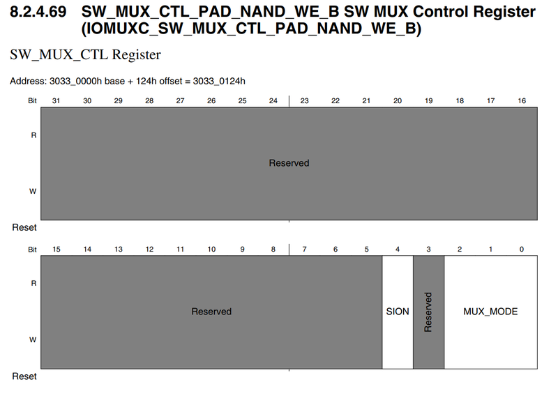
SW_MUX_CTRL register sets the multiplexing mode of the pin. Example:
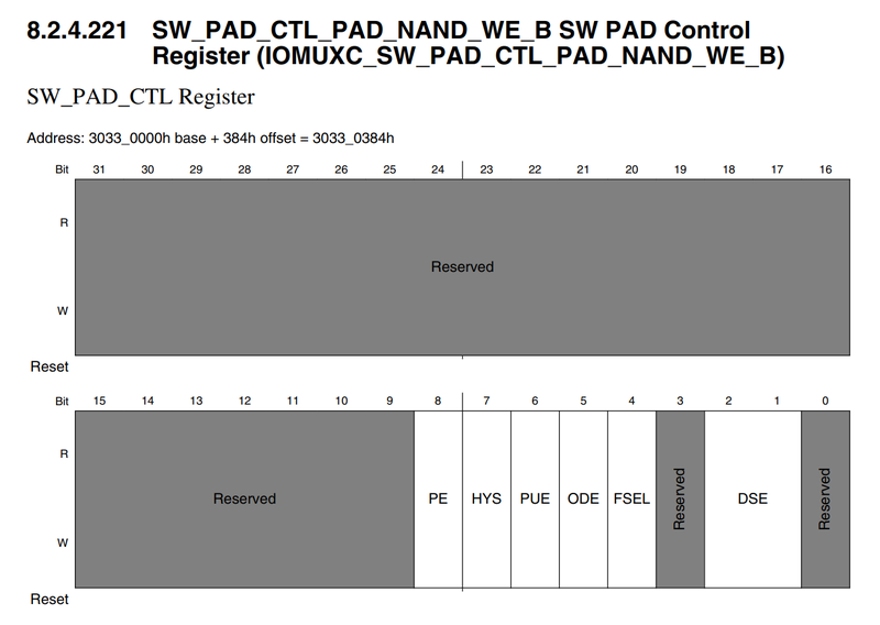
SW_PAD_CTRL register sets the specific operating setting of the pin. Example:
Example: adding a gpio_led node
In this example, the fsl,pins has one pin entry: pin MX8MP_IOMUXC_NAND_READY_B is configured for function GPIO3_IO16.
&iomuxc {
	pinctrl-names = "default";
	pinctrl-0 = <&pinctrl_hog>;

	pinctrl_hog: hoggrp {
		fsl,pins = <
			MX8MP_IOMUXC_HDMI_DDC_SCL__HDMIMIX_HDMI_SCL	0x400001c3
			MX8MP_IOMUXC_HDMI_DDC_SDA__HDMIMIX_HDMI_SDA	0x400001c3
			MX8MP_IOMUXC_HDMI_HPD__HDMIMIX_HDMI_HPD		0x40000019
			MX8MP_IOMUXC_HDMI_CEC__HDMIMIX_HDMI_CEC		0x40000019
		>;
	};
	pinctrl_gpio_led: gpioledgrp {
		fsl,pins = <
			MX8MP_IOMUXC_NAND_READY_B__GPIO3_IO16	0x19
		>;
	};
...
}
Interface Configuration Examples
UART
Pinmux
pinctrl_uart2: uart2grp {
	fsl,pins = <
		MX8MP_IOMUXC_UART2_RXD__UART2_DCE_RX	0x49
		MX8MP_IOMUXC_UART2_TXD__UART2_DCE_TX	0x49
	>;
};
Device Node
&uart2 {
	/* console */
	pinctrl-names = "default";
	pinctrl-0 = <&pinctrl_uart2>;
	assigned-clocks = <&clk IMX8MP_CLK_UART2>;
	assigned-clock-parents = <&clk IMX8MP_SYS_PLL1_80M>;
	status = "okay";
};
GPIO
For GPIOs to be used directly by user space applications:
Pinmux
pinctrl_uart3: uart3grp {
	fsl,pins = <
		MX8MP_IOMUXC_UART3_RXD__GPIO5_IO26	0x49 /* GPIO=(5-1)*32+26=154 */
		MX8MP_IOMUXC_UART3_TXD__GPIO5_IO27	0x49 /* GPIO=(5-1)*32+27=155 */
	>;
};
| These pinmux group must be configured by iomux driver. |
&iomuxc {
	pinctrl-names = "default";
	pinctrl-0 = <&pinctrl_hog> <&pinctrl_uart3>;
...
}
For GPIOs to be used as peripheral control signals (reset, interrupt, power control etc.)
Pinmux
pinctrl_flexcan1_reg: flexcan1reggrp {
	fsl,pins = <
		MX8MP_IOMUXC_GPIO1_IO00__GPIO1_IO00	0x154	/* CAN1_STBY */
	>;
};

pinctrl_flexcan2_reg: flexcan2reggrp {
	fsl,pins = <
		MX8MP_IOMUXC_GPIO1_IO01__GPIO1_IO01	0x154	/* CAN1_STBY */
	>;
};
Device nodes
	reg_can1_stby: regulator-can1-stby {
		compatible = "regulator-fixed";
		regulator-name = "can1-stby";
		pinctrl-names = "default";
		pinctrl-0 = <&pinctrl_flexcan1_reg>;
		regulator-min-microvolt = <3300000>;
		regulator-max-microvolt = <3300000>;
		gpio = <&gpio1 0 GPIO_ACTIVE_HIGH>;
		enable-active-high;
	};

	reg_can2_stby: regulator-can2-stby {
		compatible = "regulator-fixed";
		regulator-name = "can2-stby";
		pinctrl-names = "default";
		pinctrl-0 = <&pinctrl_flexcan2_reg>;
		regulator-min-microvolt = <3300000>;
		regulator-max-microvolt = <3300000>;
		gpio = <&gpio1 1 GPIO_ACTIVE_HIGH>;
		enable-active-high;
	};
SPI
Pinmux
pinctrl_ecspi2: ecspi2grp {
	fsl,pins = <
		MX8MP_IOMUXC_ECSPI2_SCLK__ECSPI2_SCLK		0x82
		MX8MP_IOMUXC_ECSPI2_MOSI__ECSPI2_MOSI		0x82
		MX8MP_IOMUXC_ECSPI2_MISO__ECSPI2_MISO		0x82
	>;
};

pinctrl_ecspi2_cs: ecspi2cs {
	fsl,pins = <
		MX8MP_IOMUXC_ECSPI2_SS0__GPIO5_IO13		0x40000
	>;
};
Device Node
&ecspi2 {
	#address-cells = <1>;
	#size-cells = <0>;
	fsl,spi-num-chipselects = <1>;
	pinctrl-names = "default";
	pinctrl-0 = <&pinctrl_ecspi2 &pinctrl_ecspi2_cs>;
	cs-gpios = <&gpio5 13 GPIO_ACTIVE_LOW>;
	status = "okay";

	spidev1: spi@0 {
		reg = <0>;
		compatible = "rohm,dh2228fv";
		spi-max-frequency = <500000>;
	};
};
I2C
This example shows three I2C devices configured on I2C bus #2.
Pinmux
pinctrl_i2c2: i2c2grp {
	fsl,pins = <
		MX8MP_IOMUXC_I2C2_SCL__I2C2_SCL			0x400001c3
		MX8MP_IOMUXC_I2C2_SDA__I2C2_SDA			0x400001c3
	>;
};
Device Node
&i2c2 {
	clock-frequency = <400000>;
	pinctrl-names = "default";
	pinctrl-0 = <&pinctrl_i2c2>;
	status = "okay";

	eeprom@50 {
		compatible = "atmel,24c08";
		reg = <0x50>;
		pagesize = <16>;
	};

	eeprom@54 {
		compatible = "atmel,24c08";
		reg = <0x54>;
		pagesize = <16>;
	};

	rtc@69 {
		compatible = "ab1805";
		reg = <0x69>;
		pagesize = <16>;
		status = "okay";
	};
};

